AFM & NSOM
>>SPM Accessories®
Related Products
SPM-M Kit
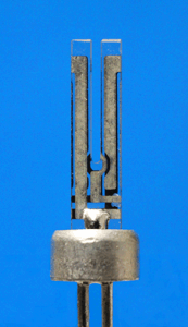
Tuning Forks
MMP Series
MadPLL®
Nano-MET10 & Nano-MET20
Nano-METZ
Nano-METSeries
Nano-SPM200
Nano-LPQ
Nano-HS3M
SPM-MZ
Nano-OP Series
Nano-OPH Series
Nano-P Series
Nano-LR200
Nano-CZ200
Nano-CZ500
Nano-HSZ
Nano-MZ
Nano-Bio Series
Nano-H Series
Nano-PDQ Series
Nano-T Series
Nano-HS Series
Nano-M250
Nano-LP Series
Nano-M350
Nanopositioning Accessories
Nano-Drive®
Questions?
E-Mail Us |
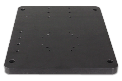
SPM baseplate
Anodized aluminum plate, dimensions 10.75 in. x 8 in. x 0.5 in, compatible with Mad City Labs manual and motorized micropositioning XY stages for SPM as well as the SPM-MZ. Additional 1/4-20 tapped holes on 1 inch spacing for accessories.

|
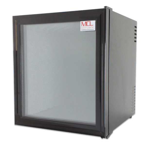
Double insulated enclosure
Exterior dimensions approximately 20 in. high, 17 in. wide, and 19 in. deep. Interior dimensions approximately 15 in. high, 12 in. wide, and 10.5 in. deep. Glass door and double insulation for thermal isolation. Door has recessed handle and is reversible.

|
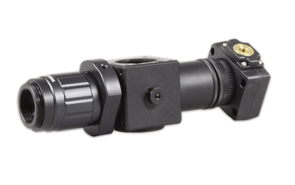
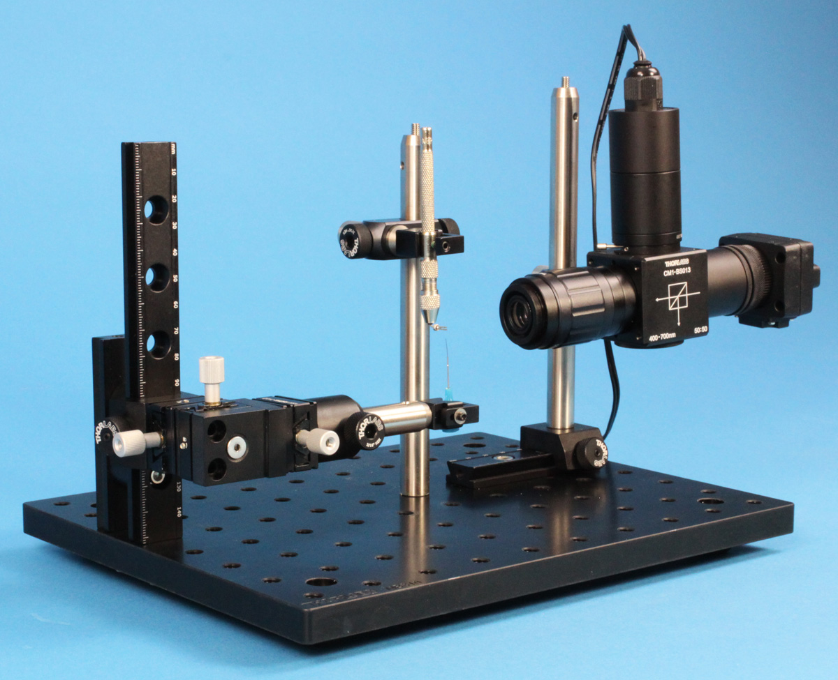
Video Optical Microscope
Suitable for visualizing approach of SPM probe to sample surface. Microscope output to USB2.0. Manual XYZ positioning capability included. Video screen not included.

|
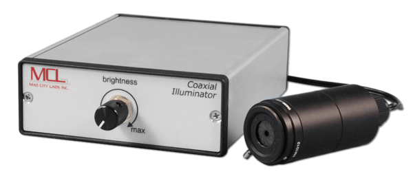
Coaxial Illuminator
Adjustable output, white LED illumination for use with the Video Optical Microscope.

|
SPM Etch Kit
The Mad City Labs SPM etch kit is designed allow users to create a sharp tungsten tip suitable for scanning probe microscopy. The instrumentation allows the user to attach a tungsten wire to a quartz tuning fork and electrochemically etch the wire. The attachment of the wire is done with the assistance of a three axis manual micropositioner and video optical microscope. The etching process uses the lamella method where the wire passes through a thin lamella and into a bath of potassium hydroxide(KOH) or sodium hydroxide (NaOH). A bias voltage is applied to the electrodes in the film and bath which causes the tungsten wire to be etched by the film. When the wire is completely etched, the bottom portion of the wire falls, the etching process is complete, and the remaining top portion of the wire is left with a very sharp tip.

|
Parts
- Coaxial illuminator
- Video optical microscope (1x magnification, 50mm)
- Tip etching station controller and LabVIEW based software
- 5 large tuning forks
- Baseplate
- Rails, stainless steel posts, 3 axis manipulator.
|
|
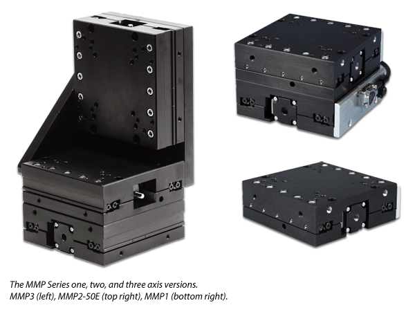
Nanopositioner-ready, stepper motor driven, micropositioning systems with 1, 2, or 3 axes for high precision positioning for a variety of applications.

|
Recommended Nanopositioners and Micropositioners for AFM & NSOM
| Product |
Description |
Applications |
SPM-M Kit
|
High resolution, closed loop, scanning resonant probe microscope |
nanoscale characterization, nanoscale fabrication, optical antennas, nano-optics, semiconductors, data storage, and more |
MadPLL®
|
Fully integrated instrument package that allows the user to create a low cost, closed loop, "instant" AFM or NSOM |
AFM and NSOM |
Nano-MET10 & Nano-MET20
|
High speed, ultra-low noise system with ranges of motion 10 µm or 20 µm |
high speed, high resolution positioning, Metrology, AFM, SPM |
Nano-METZ
|
High speed, ultra-low noise system with range of motion 5 µm |
high speed, high resolution positioning, Metrology, AFM, SPM |
Nano-MET Series
|
High speed, ultra-low noise system with ranges of motion 75 µm (XY) and 5 µm (Z) |
high speed, high resolution positioning, Metrology, AFM, SPM |
| Nano-SPM200 |
Compact nanopositioning system with 200µm travel |
AFM, NSOM, SPM, nanofabrication |
Nano-LPQ
|
Ultra-low profile, high speed nanopositioning system with 75 microns of travel in XY and 50 microns of travel in Z |
optical trapping, optical tweezers, high speed particle tracking, NSOM, SPM |
Nano-HS3M
|
High speed, ultra-low noise system with range of motion 10 µm (XY) and 5 µm (Z) |
high speed, high resolution positioning, Metrology, AFM, SPM |
SPM-MZ
|
Precision aligned, highly stable single axis micropositioner designed as a Z-axis approach for scanning probe microscopes. |
scanning probe microscopy, nanomanipulation |
Nano-OP Series
|
Ranges of motion from 30 µm up to 100 µm and can be combined to provide multi-axis motion |
AFM, NSOM, interferometry, optical fiber positioning |
| Nano-OPH Series |
Large central aperture, ranges of motion from 30 µm up to 100 µm |
nanomanipulation, AFM, NSOM, specialized microscopy |
| Nano-P Series |
Precision linear translator in a small cylindrical configuration with 15 µm, 35 µm or 70 µm of motion |
metrology, AFM, NSOM, SPM, nanoindenting |
| Nano-LR200 |
200 µm of motion combined with exceptionally low out-of-plane motion for special applications |
AFM, SPM, NSOM, wafer profilometry, optical alignment |
| Nano-CZ200 |
Compact, long range (200 µm) precision nanopositioning system |
metrology, high precision optical alignment and mirror positioning, scanning probe microscopy |
| Nano-CZ500 |
Compact, super long range (500 µm) precision nanopositioning system |
high resolution probe scanning, metrology, optical alignment and mirror positioning |
| Nano-HSZ |
High speednanopositioner with picometer precision |
high speed AFM, NSOM, SPM, optical alignment and miror positioning |
| Nano-MZ |
Compact with 25 µm range of motion |
AFM, optical aligment, metrology |
| Nano-Bio Series |
Low profile, with large aperture for use with inverted optical microscopes, available in 50 µm, 100 µm, and 200 µm ranges of motion |
optical microscopy, AFM scanning, super resolution (SR) microscopy |
| Nano-H Series |
Compact, long range stage with a large aperture |
optical microscopy, AFM scanning, fluorescence imaging, optical tweezers |
| Nano-PDQ Series |
Extremely high speed nanopositioners with a large center aperture, up to 75 µm of motion in XY, and 50 µm of motion in Z |
optical trapping, optical tweezers, high speed particle tracking, AFM, NSOM |
| Nano-T Series |
Economical systems with sub-nanometer resolution |
fluorescence imaging, super resolution (SR) microscopy, AFM scanning |
| Nano-HS Series |
High speed nanopositioning system with picometer positioning resolution |
high speed AFM, SPM, metrology |
| Nano-M250 |
Compact system constructed from titanium or invar with a 0.5 inch aperture |
nanolithography, SEM, AFM |
| Nano-LP Series |
Low profile with 100µm, 200 µm or 300 µm in X, Y and Z. |
single molecule microscopy and spectroscopy, AFM scanning, fluorescence imaging, super resolution (SR) microscopy |
| Nano-M350 |
Compact, constructed from titanium and aluminum with a 0.25 inch aperture |
nanolithography,SEM, MEMS testing, alignment, AFM |
|
AFM Demonstrations
Position noise of a nanopositioning system is the ultimate limit of the system's measurement resolution. Many applications involving sub-nanometer measurements, such as atomic force microscopy (AFM), would not be possible without low noise nanopositioning systems. Some companies claim to sell systems with sub-nanometer resolution, but they do not have data from external metrology tests to support their claims. All Mad City Labs nanopositioning products are rigorously tested before shipment. These tests involve a series of measurements designed to fully characterize the performance of the nanopositioning system with a realistic environment and testing conditions that match the application. Available metrology tools include NIST-traceable interferometers, high resolution AFM, and a high resolution position noise analyzer, designed specifically for nanopositioning characterization. The links below lead to in-depth descriptions of some of our AFM measurements.
 |
|
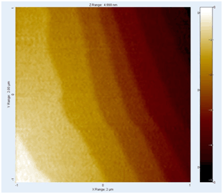
312 pm Si (111) atomic steps detected using a nanopositioner with PicoQ® sensor technology, measured by AFM.
|
Measuring Atomic Steps
Measurements taken with an AFM show that nanopositioners with PicoQ® sensor technology have sufficiently low position noise to accurately resolve single atomic layer size steps, 312 pm.
Sub-Nanometer Motion
100 and 450 micron range nanopositioners with PicoQ® sensor technology perform 860 picometer steps, 1 nanometer sine wave, and repeated 95 picometer steps, externally measured by AFM.
Measuring Surface Roughness
AFM is used to externally verify that the position noise of a nanopositioning system with PicoQ® sensor technology is less than the surface roughness of a Si (111) sample, 60 pm RMS.
|
|


